

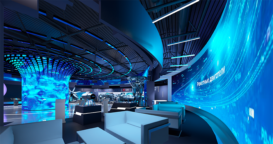
In this era of rapid technological advancement, every second introduces new innovations that subtly reshape our world. LED displays, integral to our daily lives from outdoor billboards to home theaters and concert venues, are omnipresent, showing off their allure. But did you know? As demands for better picture quality, brightness, and durability increase, traditional LED packaging technologies are struggling to keep up. Enter MIP (Mini LED display wall / Micro LED Display In Package) technology — akin to outfitting LED screens with a "super suit," this technology levitates the display quality to new heights!
What is MIP Packaging Technology?
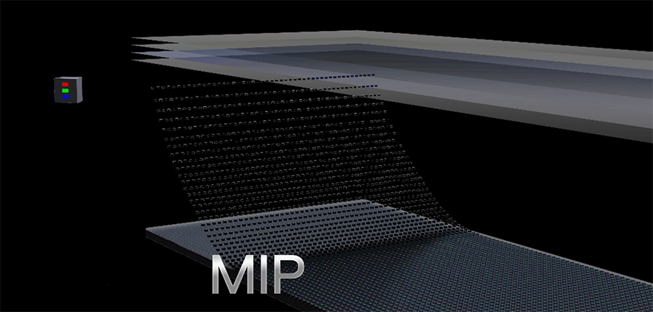
MIP, standing for Mini LED display wall / Micro LED Display in Package, is an advanced LED packaging method that merges the high performance of Mini LED display wall / Micro LED Display chips with the precision of packaging craft. This union brings revolutionary changes to LED displays. Here’s a deeper look into the principles of MIP technology:
Principles of MIP Packaging Technology:
1. Mass Transfer of Chips:
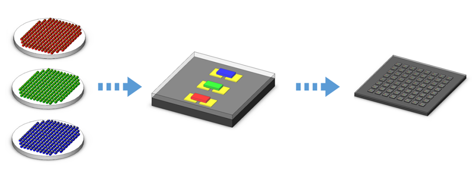
The first step in MIP technology involves transferring Micro LED chips onto a substrate using mass transfer technology. This precision method allows for moving numerous tiny LED chips from a growth substrate to another substrate (like a PCB), maintaining high yield rates and accurate positioning essential for dense LED arrays.
2. Chip Packaging:
Once transferred, the Micro LED chips are packaged on the substrate. This includes affixing the chips with conductive or non-conductive adhesive and making electrical connections through wire bonding. The packaging materials not only protect the chips from external conditions but also assure effective heat dissipation, ensuring stable operation of the LED chips.
3. Cutting into Smaller Packages:
The large area LED array that has been packaged is then cut into smaller units. These units could be individual LED chips or groups of chips forming a module. Precision equipment is necessary in this stage to ensure each unit meets specific size and shape requirements.
4. Spectrum Mixing:
After cutting, the smaller units undergo spectrum mixing, which controls the light emitted by each LED chip to ensure uniformity and consistency in the display’s color quality. This is a crucial step for achieving high-quality displays.
5. Surface Mount Technology and Cover Film Application:
Finally, the spectrally mixed units are mounted onto the display’s back panel and finished with a cover film appliance. High precision is again required to position each unit correctly and smoothly on the panel. The cover film provides additional protection and enhances the aesthetic appeal.
Through these detailed steps—from chip transfer and packaging to cutting, spectrum mixing, and final assembly—MIP technology elevates LED displays to a level of superior performance and quality. This innovation rejuvenates the LED display industry with new vitality.
Advantages and Limitations of MIP Packaging:
Advantages of MIP Packaging Technology:
Exceptional Display Quality:
MIP technology enables full measurement and precise spectral comparison of Micro RGB pixels, offering superb performance in terms of brightness, contrast, and color consistency across different viewing angles. This significantly enhances the display quality, providing users with a more lifelike visual experience.
Low Maintenance Needs:
Should LED beads fail, MIP technology allows them to be individually replaced without affecting other parts of the screen, simplifying maintenance and reducing costs. Additionally, it offers excellent protection against dust, moisture, and static electricity, enhancing the device's stability and reliability.
Cost-Effectiveness:
Scalable manufacturing of MIP technology helps in reducing wafer costs, lowers defect rates, and cuts back on downstream rework expenses. Compatibility with existing equipment also avoids the costs associated with buying new machines and R&D investment, giving MIP technology a competitive edge in cost management.
Flexibility and Compatibility:
MIP technology can reuse SMD production equipment, limiting heavy asset investments. It adapts to different pixel pitches, offering high flexibility, and is compatible across various applications.
Excellent Heat Dissipation:
LED modules with MIP packaging exhibit improved heat dissipation, crucial for reducing power consumption and operational heat, significantly enhancing device stability and lifespan.
Challenges with MIP Packaging Technology:
Technological Maturity:
While packed with advantages, MIP technology still may need to catch up in maturity compared to traditional packaging methods. This includes overcoming challenges in mass transferral and color splitting, which require ongoing R&D and optimization.
Market Acceptance:
As a burgeoning technology, MIP may need time to gain full market acceptance. Potential users need time to recognize its benefits and applicative value.
Cost Competitiveness:
In certain high-end applications, the cost benefits of MIP technology might not be immediately evident. More efforts are needed to reduce costs and enhance cost-performance ratios relative to established packaging technologies.
Application Limitations:
Although MIP technology excels in small-pitch and mini-pitch LED display domains, it may still face challenges in specific scenarios requiring extremely high pixel density or unique optical effects. In such cases, MIP might need to be combined with other technologies to meet requirements.
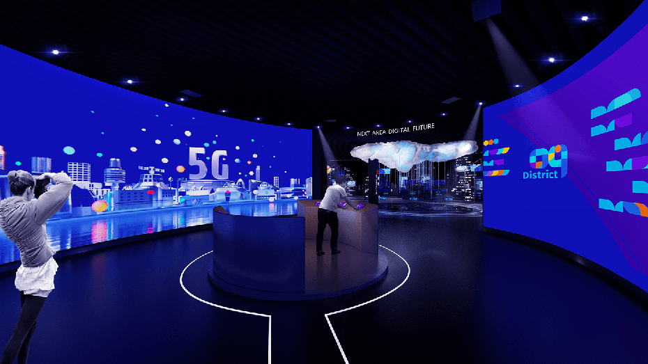
As MIP technology continues to evolve and expand its market presence, it is poised to play a more significant role in the LED display arena. With ongoing technological advancements and cost reductions, MIP technology could soon become the mainstream in LED display markets, transforming our world through enhanced technological beauty and reliability.